1. Project Overview
|
The
purpose of the circuit designed in this project is to be able to display my own
birth date using sequences of three on/off switches, producing seven outputs,
one for each LED on a seven segment display.
My only constraints are to include a resistor for each output, “a” to
“g” in the display and to use Karnaugh mapping as well as Boolean algebra to
create all of the equations. Below, I
will give a report on how my project was produced, as well a description
for each step in the process.
|

|
2. Truth Table
Below is
the truth table that I created to correspond with the numerical digits in my
birth date. Each number has a set of
LEDs, “a” to “g”, in its display that are either on or off to show the
number.

For each
set of inputs, the LEDs are set up to a point where when that sequence is in,
the subsequent lights will flash displaying that number. The “x” in the last two columns is meant to
show that they do not have any effect on the circuit. In this case, I only needed to use six digits
out of the eight available to show my birth date, so the Boolean sequences 110
and 111 do not mean anything.
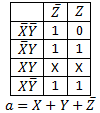
3. Karnaugh Maps and Simplified Logic
|

|

|

|

|

|

|
Above are
the Karnaugh maps that I have used to make the simplification of my expressions
exponentially easier. For each LED, I
must create an equation that will display which cases, or digits, it will be
lit. The ones and zeros of each scenario
are put into the map based on the formation of inputs on the outside. Then, there are methods of grouping the ones to
create minterms in a Sum of Product form.
The groups are basically producing the cases that the input is the same
throughout, or finding what is in common between them. This method is immensely efficient,
considering the time and effort saved by using this quick process. As said before, the reason for having seven
expressions is because each LED has to either turn on or off for all six
scenarios.
4. MultiSim Implementation

Above
is a picture of the circuit I created on the software MultiSim. It uses a bus to easily and cleanly display
the paths that the wires take to create the outputs of the seven segment
display. All of the different groupings
of gates represent the seven LEDs, but I only needed to create four circuits
because the “d” and “e” lights have the same equations, “b” is always on, and
the “c” and “f” lights have the same equations.
All together, I have three inverters, four OR gates, one NOR gate, and
two NAND gates. Therefore, I only need
one inverter, one OR, one NAND, and one NOR integrated circuit. The reason why I use NAND and NOR gates is to
efficiently make my circuits more organized.
I have figured out which type of gates to use between the three
available cases to create a circuit with the least amount of integrated
circuits. Instead of using 14 different
gates and five integrated circuits for the AOI design, I only have to use 10
gates and four integrated circuits with my current system. This cuts down on the space and materials
needed to create the bread boarding. Now
the seven segment display works in a way based on the type being used. I am using a common cathode display, which takes in a VCC power as a 1 value to turn on the LED because on the other end is a ground connection. A common anode display is the exact opposite, needing a ground connection to go with its power extension to create a 1. As said before, I am using the common cathode display. This is because the switches and circuits that I have set up create a 1 by applying a power input. The reason for adding resistors is to prevent the LEDs from blowing the circuit.
5. Bill of Materials

This is a bill of materials, used to organize the materials I will need to produce the breadboard. It shows how many integrated circuits I will need so I could compare it to the other form of circuits.
6. BreadBoarding

The materials needed
|
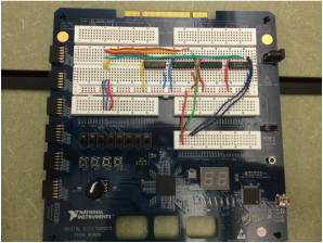
A semi-finished product
|

The working circuit
|
These pictures are visual displays of the series of steps I took to create a successful circuit. In the first picture, I have shown that I set up a method of organization to ensure that my process is as easy as possible. In the second picture, I have created approxiamately 75% of the MultiSim design. For example, through the use of first the 74LS04N "NOT" integrated circuit, then the 74LS32N "OR" gate, I created the "a" LED. The "g" LED only needed to use OR gates, and the other gates, NAND and NOR, are used once each for four different LEDs. The third picture is a completed board displaying the inputs 011 that sends a 1 to a, b, c, f, and g to broadcast a nine. Overall, my experience with breadboarding this project was smooth sailing compared to my first one. I only made one mistake, being the orientation of the NOR integrated circuit. Both the OR and NAND chips have two inputs and an output going from left to right, where as the NOR is from right to left. The NOT holds two more outputs because they only take in one input. These facts are important when producing a prodcut with multiple chips.
7. Final Project Conclusions
In conlcusion, this is almost a mirror image of the prior project, except with the addition of NAND gates, NOR gates, and Karnaugh mapping. After doing almost the same thing again, I have a more experienced approach towards making a successful circuit. I am sure to create a steady method of organized circuitry that allows me to easily trouble shoot. For example, I color cordinated the circuit so that any "hot" colors (red, orange, and yellow) are part of the AOI design, while the NOR design uses "cooler" colors (green and blue). If I were to do this same project again, I would create a design that used the least amount of integrated circuits, not gates. What I was doing was choosing a design that uses the less amount of chips per LED, but that may cause them to add up as a whole display. This time, using the Karnaugh mapping has allowed the process of simplifying all seven segments to quicken in pace, where as in the last project, I had to simplify one epression with several lines of Boolean Algebra. To sum it up, I enjoyed this project much more than the other and would recommend it in the future.
Extra Credit Documentation

|


|
